Samsung to mass produce Nano 2 generation D ram… 2 years ahead of competitors
Park Jung Il | comja77@ | 2017-12-21 10:36:27

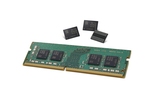
2 generation 10 nano degree D ram of Samsung Electronics and D ram module to be applied.
Samsung Electronics once again broke the limits of micro-fabrication. The company is firmly in the position of a strong player in the memory semiconductor market with a `super-gap` strategy that widens technology gap with competitors.
Samsung Electronics, on December 20, revealed that it started mass production of 1y nano (mid-10nm) DRAM, the world`s first 10nm-class second generation, from last month. It is only 21 months since the mass production of 1x nano (late 10nm) DRAM, which is the first generation of 10nm-class in February last year.
Samsung Electronics stated that it increased its productivity by about 30% compared to 1x nano DRAM without using next-generation extreme ultraviolet (EUV) exposure equipment. Considering that SK Hynix, the second largest maker in the industry, has mass-produced 1x nano-D RAM since last October, it showed a technology gap of nearly one year and eight months. Micron, the US maker, said it would mass-produce 1x nano-D DRAMs this year, but it has not been confirmed whether it will mass-produce it.
Samsung Electronics plans to increase the proportion of 1x nano DRAM production to more than 50% this year, and gradually increase 1y DRAM according to market conditions. It plans to mass-produce all the DRAMs except for some special DRAMs in 10nm process.
Samsung Electronics said it has applied three innovative processes to its products: ultra-fast, power saving, small circuit design, ultra-sensitive cell data sensing system design, and second-generation air gap process. Ultra-sensitive cell data sensor technology is an ultra-precise voltage difference detection system that can read data stored in a cell more precisely and improve the read characteristic more than double.
The air gap is a process of making the insulation layer around the current-carrying line without filling the space with a separate insulating material and making the space completely empty. Air has higher insulation efficiency than other materials and has the advantage of increasing the degree of integration of the cell array, but the structure is mainly used for simple NAND flash because of the high degree of process difficulty.
The company said the speed was 10 % faster than that of the first-generation 10-nanometer DRAM, saving more than 15 percent in power consumption. A company official said, "The design and process have changed drastically compared to the first generation, and we expect it to become a game changer for the DRAM industry."
Samsung Electronics said it has secured the basis for mass production of next-generation premium DRAMs such as DDR5 for servers based on the innovative process technology developed by Samsung Electronics,, LPDDR5 for mobile, HBM3 for supercomputers, and GDDR6 for high-speed graphics.
"We will break the technological limitations of semiconductor technology with innovations in innovation," said Jeong Kyoong-young, president of the memory division of Samsung Electronics. "We will increase the competitiveness of the super-gap by shifting the premium DRAM market to 10nm "He stated.
By Park Jung Il comja77@
