

Samsung to produce the first 10 nanometer DRAM in 2019
[ Park Jung Il comja77@ ] | 2017-11-29 10:00:58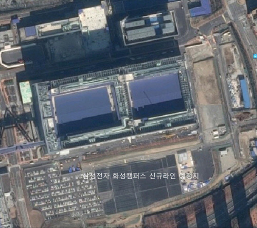
Samsung Electronics Electronics production line for EUV exposure equipment in Hwasung Semiconductor Complex Powered by Google Earth
Samsung Electronics is planning to construct a dedicated production line for EUV exposure equipment in the Hwasung semiconductor factory complex in Gyeonggi-do, and is likely to produce a next-generation DRAM that uses micro-processes at the beginning of 2019 . In the DRAM market, which continues to boom, we believe it will secure profitability while simultaneously widening gap between microprocessor technology and competitors.
According to industry sources, Samsung Electronics plans to start construction of a new line for EUV next month when it reaches the parking lot around the 17th line of Hwaseong Complex, and will install several EUV and clean room equipment and start operation from 2019. It is reported that the EUV exclusive line is under consideration by linking it with seven existing semiconductor production lines and a conveyor belt. Samsung Electronics` Hwaseong Semiconductor Complex has DRAM and NAND flash as well as a foundry (semiconductor commissioning) line.
It seems that Samsung Electronics will use EUV for not only foundry (semiconductor commissioning) process but also memory semiconductor such as DRAM. Samsung Electronics is expected to be the first in the industry to produce DRAMs in the first 10 nanometers in 2019 using EUV.
Currently, exposure equipment that draws semiconductor circuit lines uses 193 nm ArF excimer laser and liquid immersion. The physical line width is 38 nm. In order to overcome this, we have strengthened the micro process by dividing the circuit pattern two or three times, but it is difficult to implement 10-nm or less DRAM. EUV exposure equipment can significantly reduce circuit linewidth by using a shorter wavelength of 13.5 nm than visible light, thus enabling fine processing below 10 nm.
Recently, Hwaseong City passed a deliberation on the traffic impact examination for Samsung Electronics` production line expansion. As a result, Samsung Electronics is expected to go into the expansion soon after passing administrative procedures such as remaining licenses and permits.
"EUV is basically used for 7nm process, but some can be used for DRAM production," said an industry observer who is familiar with Samsung Electronics. "However, as the wafer production speed is slower than the existing patterning photo process, The key is whether we can find a way to do it. " Samsung did not disclose exactly how many EUV equipment to install. However, according to the industry, 4 ~ 8 units will be installed.
Samsung Electronics is using a double-quad patterning process that draws multiple layers of circuitry from existing exposure equipment to 18-nanometer DRAMs, which have been in production since October of last year. Although Samsung Electronics has already prepared the technology for mass production of 10-nano-sized DRAM, it is known that the industry is considering a time to introduce EUV. The EUV, which is produced exclusively by the Netherlands ASML, is advantageous for drawing ultrafine linewidths, but it has the disadvantage of costing tens of billions of dollars per unit and slowing the processing speed.
Samsung Electronics is also considering the use of EUV in the production of 10-nano DRAMs, which is believed to maintain its dominance in the mobile DRAM market. According to market researcher DRAMExchange, Samsung Electronics` share of the mobile server DRAM market in the third quarter is 58.3% and 45.9%, respectively, which is higher than the total DRAM market share of 45.8%. Samsung`s 3Q operating profit margin is 62%.
Competitors such as SK Hynix are facing similar problems. SK Hynix plans to begin late-10-nm DRAMs in the fourth quarter of this year, and plans to complete DRAM research and development in the middle of next 10-nanoseconds later in the latter half of next year. However, Hynix has spoken of its plan to introduce EUV.
By Park Jung Il comja77@
